
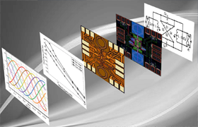
Hardware Design
The Electronics design team has got expertise in High speed Electronics, Analog as well as mixed signal , Microprocessor and micro contrlollers, RF and High frequency as well as Power Electronics. The proven basic building blocks make it easy and faster to come up with new designs. The team is well aware of the complexities associated with Optoelectronic controls, thermal aspectas well as signal integrity. All the designs are done taking into account the life expectancy of the components,ESD and EMI/EMC requirements.
Firmware Development
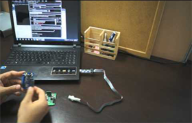
The expertise in embedded system covers requirement analysis, specification development and implementation, integration of embedded software, application and system programming, graphical user interface as well as interface and protocol development. The team is fully conversant with the state of the art chips, and coding is done as per the industry standards. The developed firmware ndergoes rigorus independent testing before release.
PCB Layout Design
Our PCB design teams have specialized Engineers who are well experienced in providing Engineering data preparation services for the global PCB industry. We act as a seamless extension to your in-house facility. As your process partner, we have the size, the technical resources and the experience to learn fast your requirement, to work closely with your in-house staff, and to deliver the job accurately and on time.
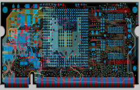
PCB design team works with clients across the globe addressing solutions for highly complex PCB design solutions meeting IPC specifications. PCB Engineering solutions include High Speed PCB Design, SI Analysis (Time Domain and Frequency Domain analysis), EMI/EMC and Reliability Analysis. The design team is well experienced in handling multi layer, complex and dense circuits. The Design for manufacturability as well as design for testing are taken care in the design itself, so that there shall be a smooth transfer to manufacturing.
Manufacturing of Electronics Printed Circuit Board Assembly
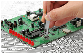
We provide high-quality PCBA services from prototyping, low volume, mid volume to mass production. Using cutting edge and advanced SMT and THT technology, we deliver high quality reliable, tested, and ready-to-use circuit board assemblies. Our 20 years of expertise lies in manufacturing of all types of PCBAs for various sectors and applications. With expert sourcing, precision assembly, and strict quality control, we help bring our clients electronics products to life. The manufacturing process follows ISO 9001:2015 and ISO13485:2016 standards as well as AS9100 Rev D for Aerospace& Deference Applications.
Optics
This is one of the core team at Vinvish and the team comprises of several PhD and Master degree holders in Optics and optoelectronics. Modeling of classical optical components and simulation of systems make it easy for optical system designs. The clean optical lab is well equipped with state of the art equipment like Vibration table, Optical Spectrum Analyser, Optical sources, Precision alignment stages and drivers, Power meters, Special purpose splicing equipments, etc.

Mechanical Design
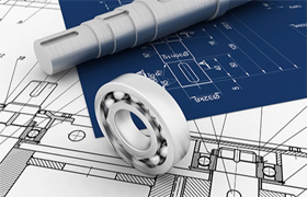
Mechanical design team uses AutoCAD as well as Solidworks CAD tool to design mechanical components and systems. The analysis done are tolerance analysis, Finite Elemement analysis, thermal analysis, etc. 2D as well as 3 D drawings are created for further manufacturing.
Manufacturing of Mechanical Parts
Vinvish Technologies Pvt. Ltd. is a leading CNC machining parts manufacturing centre, delivering high-quality machining solutions for a wide range of sectors. We specialised in producing precision-machined parts that meets the strictest dimensional tolerances and functional requirements. Our advanced CNC milling and turning centre enable us to handle everything from one-off prototypes to full-scale production with consistent accuracy and finish. The manufacturing process follows ISO 9001:2015 and ISO13485:2016 standards as well as AS9100 Rev D for Aerospace & Defence Applications.